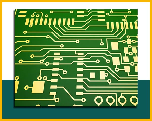
PCB DESIGN
The PCB design process employs ECAD systems and PCB software packages that enable the design and testing of the PCB schematics on both the physical and logical level. and also incorporate additional facilities in to the design, such as, simulations, complex routing and many more. The schematics for both aspects are generated and stored in digital format with frequent backups.
Capturing of circuit schematic
After the circuit schematic is developed, it has to be captured by a schematic capture tool. The capturing can be done by the PCB design software suit or by a separate software tool whose output can be exported in a suitable format. Capturing of schematic implies that the design of the circuit is contained in a file which can be converted into a netlist file. A netlist file (an ASCII file) is essentially the interconnectivity information of a circuit made of its components. The components of a PCB are generally gates, so the netlist is a connection of gates. Simulation of the circuit is also performed at this stage to learn about the design viability before going into advanced stages.
SINGLE-SIDE PCB
The single layer Printed circuit boards were first made in the year 1950, with the usage of an electronic transistor. This type of PCBs more commonly manufactured in USA, and now been in common use in majority of electronic devices in India as well. Accent Fixtures are now one of the leading companies to manufacture the single layer PCBs. By using the technique of copper etching, single layer PCBs was manufactured directly during the early time. Japan, in the period between 1953 -1955 used the imported copper make out paper phenolic aldehyde copper substrate that was used and applied mostly on the radio products. Later in the year 1956 the single layer PCB designs made a progress in the technology with its appearance in the professional manufacturing of PCBs design, this took place in Japan. The copper substrate used paper phenolic aldehyde in the early stage in Japan but due to paper
phenolic aldehyde there was poor solder thermal stability and twist issue due to its factors like low electric insulation. Soon after this paper epoxide resin and glass fiber epoxy resin was developed. In recent times the paper epoxide resin came in wide usage in the electronic field.
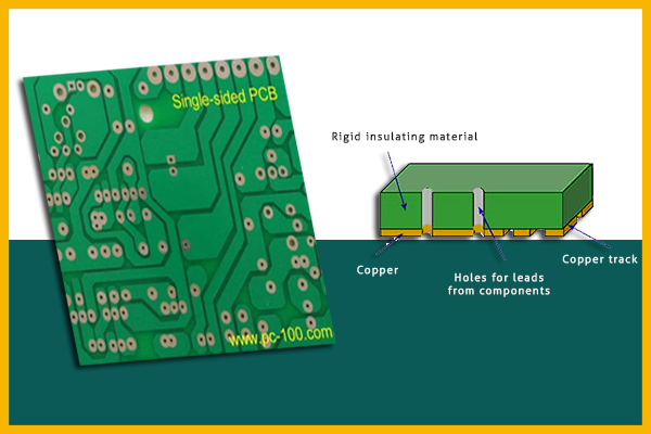
The Single layer printed circuit boards have only one layer and are also known as single sided PCBs that consist of only one layer of conductive material with best suitable low density designs. This printed circuit boards are quick in designing and easy to manufacture. They are extremely cheap and easy to maintain. Apart from the single layer printed circuit board’s simple manufacturing they are used in complex electronic devices.
Some of the examples where the single printed circuit boards are used are mentioned below;
|
|
|
|
|
|
|
|
|
|
|
|
|
|
|
|
|
|
|
|
|
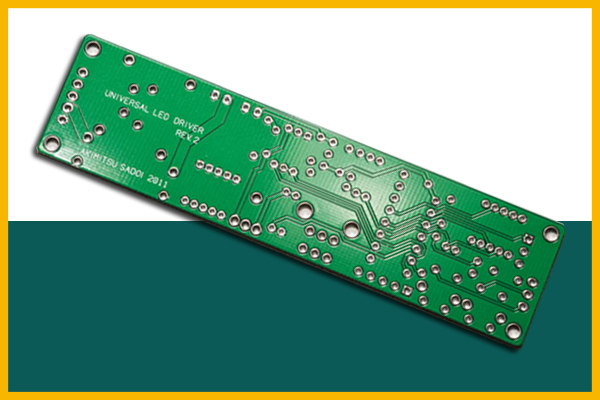
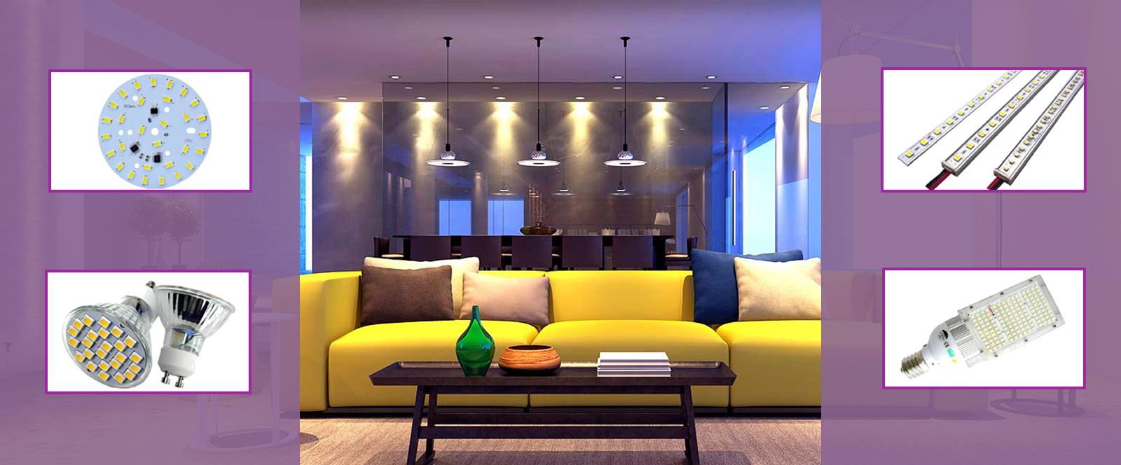
LED DRIVER PCB
We being a distinguished business company are highly dynamic in providing to the industry a vast gamut of LED Driver PCB.
 Rigid design
Long functional life
Low maintenance
High usability
Enhanced performance
Fine finish
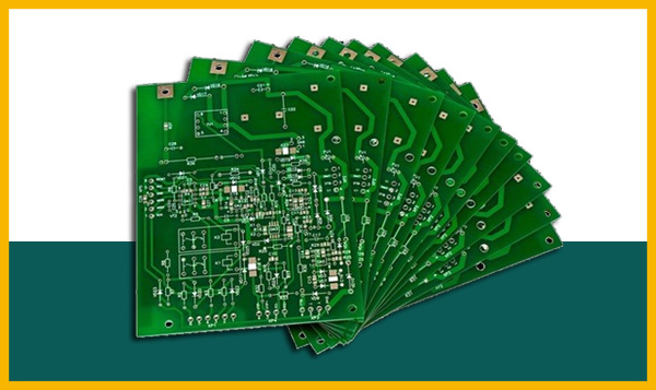
FR-4 PCB
Single Sided PCBs contain only one layer of conductive material and are best suited for low density designs. Single-sided printed circuit boards are easily designed and quickly manufactured. They serve as the most cost-effective platform in the industry. Although Single Sided PCBs are relatively simple, they can still be used in very complex devices.
Double Sided PCB
DOUBLE SIDED PCBs
Double Sided PCBs, also known as Double Sided Plated Thru or DSPT, are the most popular type of PCBs in the industry. They are like the gateway to higher technology applications. They are the two layers of the same circuit, placed on two sides interconnecting themselves through traces crossing between the sides using vias.
APPLICATION OF DOUBLE SIDED PCBs
There are near limitless applications for old and new designs. The DSPT application requirements include fine line surface mount, ultra-high copper build, high and low temperature, solder coated, Silver, and Gold finishes, and many more.
LED PCB ASSEMBLY
We can provide one-stop overall solutions for LED lighting customers including OEM, ODM, etc.